- English
- فارسی
Point-defects

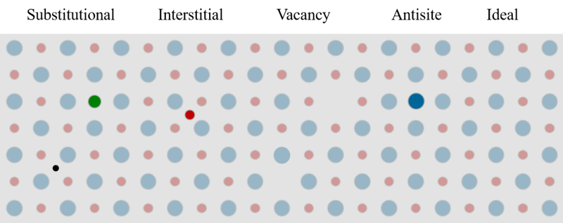
Semiconductors are the basis for the development of important technologies including microelectronics, optics, photonics, and emerging quantum technologies. Therefore, understanding, controlling, and engineering the properties of semiconductors is an essential issue in the development of modern and emerging technologies. Point defects, on the one hand, are the inevitable ingredients of any natural or manufactured semiconductor crystal with nontrivial effects on the properties and performance of the system, and on the other hand, these defects are very useful to manipulate the properties of a semiconductor toward the desired applications. By doping a semiconductor crystal with different defects, one can engineer its properties and create a wide and diverse range of applications. One of the best examples is the lithium niobate crystal (LiNbO3), which can exhibit various potential applications including holography, waveguides, and frequency converters by proper doping [1].
Computational simulations based on the first-principles calculations are very suitable tools for investigating the effect of point defects on the electronic and optical properties of semiconductors. In these schemes, without the need for expensive synthesis and analysis techniques, the properties of a semiconductor crystal can be reliably evaluated in the presence of various defects, and then after identifying the desired defects, one may call for experimental productions.
[1] Arizmendi, Luis. "Photonic applications of lithium niobate crystals." physica status solidi (a) 201.2 (2004): 253-283.
